PowerSAGMonitor Part 2: Build ── From Design to Installation at the Breaker Panel
Table of Contents
The content and implementation in this article were developed and written with Claude Code, then verified and corrected by a human. In the text, “I” refers to the human, and “Claude” refers to the AI.
This blog has a comment section. You can post with a GitHub account.
Introduction #
Part 1 (Overview) introduced what you can learn from PowerSAGMonitor, a meter that sits at my home’s breaker panel and records power outages, momentary interruptions (very short outages), and voltage drops (sags). This article is Part 2 of the three-part series. It covers the build process from design to installation at the breaker panel, and the hardware troubles that came up along the way.
The division of roles is as described in Part 1: I handled deciding the direction, buying parts, soldering, case work, wiring at the breaker panel, and measurement, while Claude handled the detailed design, drawings, and procedures.
How the Work Was Organized #
The decision to build this device was made inside my ProxmoxVE project, where I had been consulting Claude about the server reboots. Since the amount of work looked large, I split it out into its own folder as the PowerSAGMonitor project and put its history under Git. The design documents and the drawing generation scripts all live in this separate repository.
Structure of the Box #
First, here is the structure of the box I built.
The case is made of resin (Takachi PF13-6-19D, Japanese) and is mounted vertically on the wall next to the breaker panel. The deeper half faces the wall, and the flat half is the front lid. The diagram shows the lid removed and the contents pulled forward.
Inside the case are two perfboards (prototyping boards with a grid of holes), one above the other. The upper one is the signal board, and the lower one is the primary board, which carries 100V. The spacing of the posts (bosses) in the case for mounting boards does not match the mounting holes of the perfboards, so I added a 2mm-thick acrylic plate in between. The acrylic plate is screwed to the bosses in the case, and the two boards are fastened to the acrylic plate with spacers. This way I did not have to drill extra holes in the case.
Two sets of wires connect to the outside. The 100V cable from the branch breaker enters through the bottom panel, and the current sensor (CT) leads enter through the top panel, each through a rubber grommet (a part that protects the edge of the hole the wire passes through). The CTs themselves are outside the case, clamped around the main wires inside the breaker panel.
Design Approach #
Three blocks #
Inside the box (the whole resin case of the device), there are three blocks.
| Block | Contents | Role |
|---|---|---|
| Sensor block | Voltage sensors ZMPT101B ×2, current sensors (CTs; parts that clamp around a wire to measure current) SR-3704-150N ×2, signal conditioning circuits (burden resistors, filters, etc., described later) | Converts the 100V voltage and the main current into isolated 0–3.3V signals |
| Controller block | nanoESP32-C6 (a board with the ESP32-C6 microcontroller) and its built-in 12-bit ADC (a circuit that converts analog voltages into numbers) | Reads the signals and does calculation, detection, recording, and sending |
| Power block | Fuses, AC-DC module ATS005A2-F050P, EDLC (electric double-layer capacitor) 5F | Makes 5V, and keeps the device running from the EDLC during an outage |
Keeping 100V on a single board #
The circuit is hand-wired on two perfboards.
| Board | What is on it |
|---|---|
| Primary board | Terminal block, fuses, voltage sensors and their current-limiting resistors, AC-DC module, EDLC. This is the only board that carries AC100V |
| Signal board | Current sensor inputs, filters, protection diodes, the circuit that makes the midpoint voltage, microcontroller |
The reason for two boards is to confine the 100V parts to one board, and pass only isolated signals to the microcontroller side. The EDLC is on the primary board, but it sits on the output (5V) side of the AC-DC module, so it never sees 100V.
Turning AC into a signal the ADC can read #
The microcontroller’s ADC can only read 0–3.3V. So the AC signal is turned into a voltage that swings up and down around 1.65V (the midpoint). The midpoint is made by halving 3.3V with two resistors of equal value and stabilizing it with a capacitor. The midpoint itself is also read by the ADC and subtracted during calculation.
For voltage, resistors (27kΩ × 2) turn the 100V into a small current of about 2mA that flows through the voltage sensor, and the current coming out the other side is turned back into a voltage with a burden resistor (270Ω). The voltage sensor is a small transformer, and this is where it is isolated from the 100V side.
Current is handled the same way. The CT outputs the main current scaled down to 1/3000, and a burden resistor (10Ω) turns that into a voltage. Even with 40A flowing in the main wire, the voltage going into the ADC only swings about ±0.19V, far less than for voltage. The burden resistor is kept at 10Ω so that the CT is used within the conditions for which its accuracy is guaranteed (burden resistor of 10Ω or less).
Choosing Parts #
Claude and I collected the specification sheets (datasheets) of manufacturers and retailers as PDFs from the web, read them, and refined the specifications. In the end we had 42 PDFs. Beyond outer dimensions and pin spacing, even small details, such as the thickness of the bosses that only appeared in a cross-section drawing of the case, were taken from the datasheets.
Many parts were swapped for others along the way.
- Voltage sensor: The first plan was to use a small power transformer as the voltage sensor. Since transformers are bulky, I proposed switching to the ZMPT101B voltage sensor, which I had found. It turned out that with the original transformer, 100V would be applied directly across the winding, so a large current would flow if it failed, and it would burn out if a broken neutral put 200V across it. The ZMPT101B, which is used with the current limited to 2mA, came out ahead and was adopted
- Microcontroller: At first, the design used a small board (XIAO ESP32C6). It only has three pins usable for the ADC, so the design added an external ADC. That external ADC was a surface-mount part with 0.65mm pin spacing, and soldering it was expected to be the hardest part of the build. When it looked like I could get a board that breaks out all the ADC pins (ESP32-C6-DevKitC-1) from another store, we switched and dropped the external ADC. However, what actually arrived by mail order was a different board (nanoESP32-C6). It had the same microcontroller module and the pins we used were the same, so the drawings were updated to match this board and I used it as-is
- Power supply: Claude’s initial plan was to add a dedicated outlet for the box next to the breaker panel and take 5V from a USB charger. That would mean two cables from the breaker panel, one for measurement and one for power, plus the work of installing a new outlet. To lower the installation cost, I asked Claude, “Can we use a power module that mounts on the board?”, and we switched to a power module available from Akizuki Denshi (a well-known electronic parts store in Tokyo’s Akihabara). After checking heat, inrush current when power is applied, distance from 100V, and so on against the datasheet, it was adopted, and only one cable needs to enter the box
The main parts are as follows.
| Part | Model | Key specifications |
|---|---|---|
| Microcontroller board | nanoESP32-C6 | RISC-V 160MHz, 8MB flash, Zigbee / Wi-Fi 6 / Bluetooth LE, 12-bit ADC |
| Voltage sensor | ZMPT101B ×2 | Small current-type transformer. Rated 2mA : 2mA, 4kV isolation |
| Current sensor (CT) | SR-3704-150N ×2 | Clamp type (opens to clamp on), turns ratio 3000:1, up to 80A |
| AC-DC power module | ATS005A2-F050P | AC100–240V → DC5V 1A, primary–secondary AC3000V for 1 minute |
| Electric double-layer capacitor | VEC5R4505 | 5F, 5.4V |
| Fuse holder | MF-563 ×3 | PCB mount, for 5.2 × 20mm glass tube fuses |
| Branch breaker | Panasonic BSHN2202 | For single-phase 3-wire branches; L1, L2, and N can be taken out on a single cable. It always cuts L1 and L2 at the same time, so the board is never left with just one side’s 100V. Added as the outlet for the box’s power wiring |
| Case | Takachi PF13-6-19D | Flame-retardant ABS, 125 × 190 × 60mm |
Here is an excerpt of the small electronic components from the design documents.
| Part | Value | Role |
|---|---|---|
| Fuses | 0.2A ×2 (for the voltage sensors), 0.5A ×1 (for the power module) | Blow if something goes wrong on the 100V side, protecting the wiring and parts |
| Current-limiting resistors | 27kΩ × 2 in series, ×2 channels | Set the current through the voltage sensor to 2mA. Split into two so that the current does not rise too much even if one fails |
| Burden resistors | 270Ω (voltage), 10Ω (current) | Turn the current coming out of the sensors into a voltage the ADC can read |
| Filters | 1kΩ + 100nF | Remove high-frequency components the ADC cannot read |
| Protection diodes | BAT43 Schottky diode ×4 | Keep the ADC inputs within 0–3.3V |
| Midpoint circuit | 10kΩ × 2 + 100µF | Makes the 1.65V midpoint |
| Charging current-limit resistor | 33Ω (3W) | Prevents a large current from flowing into the EDLC at power-on, which would make the power module shut down |
| Diodes | 1N5819 ×2 | Prevent the EDLC’s charge from flowing back, so the voltage does not drop at the moment of an outage |
| Zener diode | 5.6V (1W) | Protects the 5V circuits in case the power module’s output ever rises |
Buying Parts #
I bought the parts through a mix of mail order and stores. On September 5, I also went shopping in Akihabara.

Back in Akihabara after a long time, shopping at Akizuki Denshi Tsusho (people and other details are blurred)
The parts list (Markdown) in the design documents was the source of truth for “what to buy,” and Claude built a purchase-tracking Excel sheet from it. For each part it tracks the planned and actual quantities, cost, and status, and selecting a status changes the row’s color.
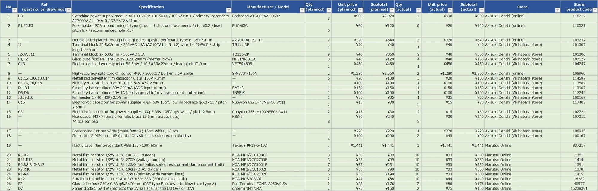
The purchase-tracking Excel sheet (partial)
When choosing parts, we made it a rule that Claude would check stock, model number, and dimensions on the product page before recommending anything. We had tripped up once over a “while stocks last” notice and over specifications that the model number alone did not determine. Also, since I enter actual costs and so on in this Excel sheet, we made it a rule that it must always be committed to Git before Claude modifies it.
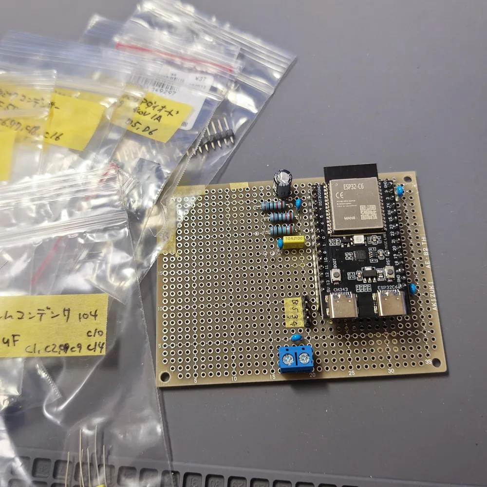
Parts were sorted into bags. On the right, the signal board as assembly begins
Generating Drawings and Documents with Python #
For the schematics, placement diagrams, and wiring diagrams, Claude generated KiCad (open-source schematic and PCB design software) files with Python scripts. Nothing was drawn in the GUI, so when the design changes, rerunning the scripts brings all the drawings up to date.
KiCad files are text inside (a nested, parenthesized format), so a program can write them directly. Claude’s Python scripts write out the schematic, placement diagram, and physical wiring layout files from a table of part positions (coordinates and orientation) and the circuit’s connections. Wiring routes are found on the grid of holes of the perfboard, a bit like solving a maze.
The resulting files are passed to kicad-cli, which runs KiCad from the command line, for checks and PDF export. There are two checks: ERC (electrical rule check), which looks for mistakes in the schematic’s connections, and DRC (design rule check), which checks whether placement and wiring violate the defined rules. Since these can be run entirely from the command line without opening the GUI, Claude can repeat “generate → check → read the violation report and fix the scripts → generate” on its own. I print the PDFs to work from, and feed the values I measure on the real parts back to Claude.
The DRC rules were rewritten for hand wiring on perfboard (keep bare wire away from other circuits’ lands, keep 100V wires 3mm away from everything else, and so on). To make sure we had not disabled so many rules that “0 violations” just meant “nothing was checked,” we also added a test that confirms warnings do appear on a drawing with deliberately inserted violations.
The physical wiring layout for the perfboard #
We were not making a printed circuit board, but I made the hand-wiring layout by reinterpreting KiCad’s layers (the layers of a board) as follows:
- Bottom copper → tinned bus wire (bare wire)
- Top copper → insulated wire
The wiring routes were also laid out automatically, and we checked the total wire length (about 2.2m in all) and the creepage distance for 100V (the distance along the surface of the insulating material). The creepage distance is watched by the custom DRC rules mentioned above. We did, however, hit pitfalls such as the entire rule file silently being disabled when a net name contained parentheses.
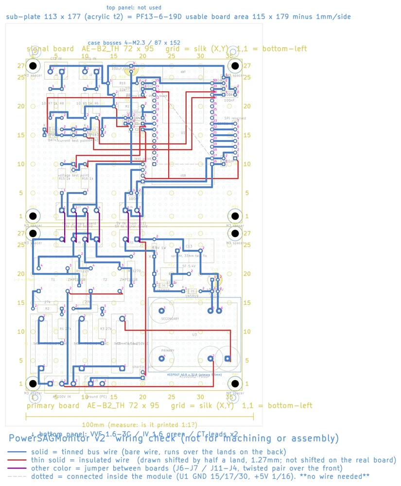
The generated wiring layout. Blue is tinned bus wire, red is insulated wire, purple is wire crossing between the boards
Here is an example of the back side that I wired based on the wiring layout and the assembly schedule. For the insulated wire on the signal board, I tried “polyurethane-coated copper wire” this time.
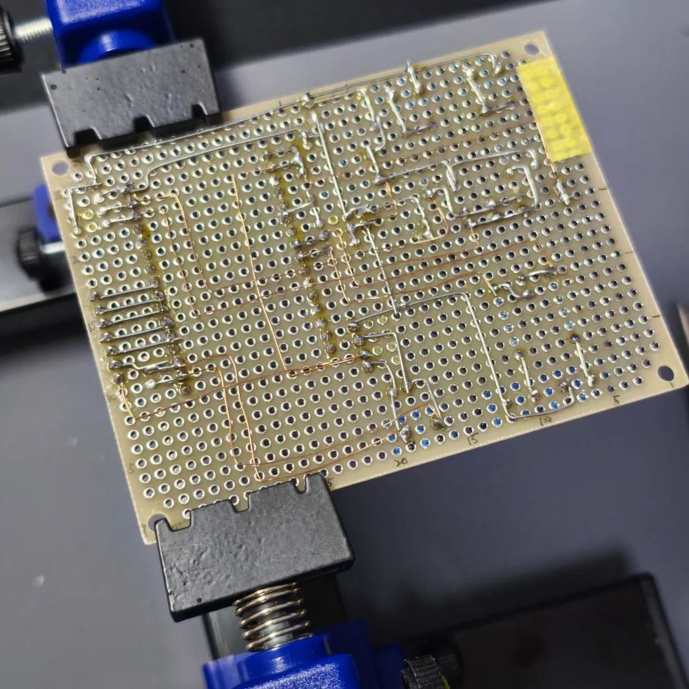
Hand wiring on the back of the signal board
I had not known polyurethane-coated wire existed. You do not need to strip it: you pass it through a blob of solder on the soldering iron where you want to connect it, and the coating melts. I had heard this makes wiring easy, but in practice it was so thin that it was hard to fix in place where I wanted it, and I did not find it especially easy. Maybe there is a knack to it.
Machining drawings #
Machining drawings were produced with the same pipeline (Python → KiCad → PDF): drilling drawings for extra holes in the boards, drilling drawings for the case, interference check drawings, cable tie position drawings, and so on. The drilling drawing for the acrylic plate can be printed at actual size on A4, and includes a 100mm verification bar to confirm that the print scale is not off.
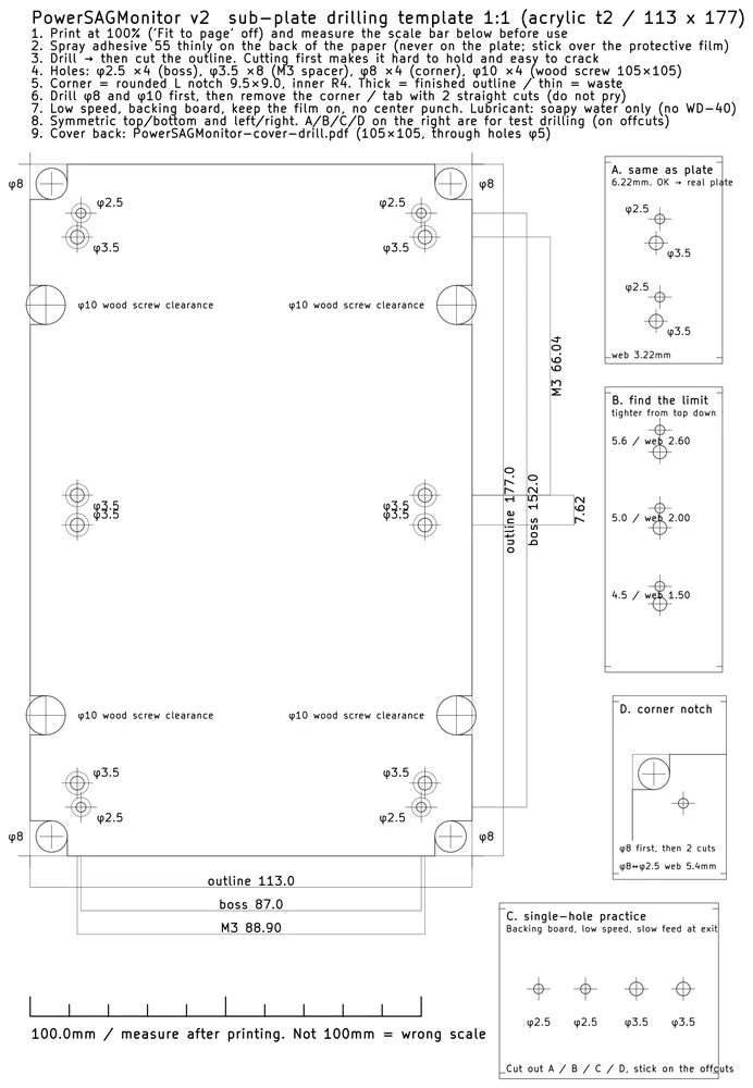
Actual-size drilling drawing for the acrylic plate
When I gave Claude the pin diameters and pitches I had measured with calipers, the number of extra holes went down from 14 to 10. In this way, the drawings were corrected with values from the real parts. Once the real device was built, we made it a rule not to rerun the generation scripts, because regenerating would make the drawings disagree with the real thing.
Assembly #
An assembly schedule that grew as I built #
Assembly followed an Excel assembly schedule made by Claude. Each row is one task, with columns such as part, coordinates, orientation, cautions, and pass criteria. I only fill in the light yellow cells (measured values, checks, notes). Pass/fail is determined automatically from the lower and upper limits. Claude reads the filled-in Excel sheet, thinks about the causes behind any NG or on-hold rows, and adds the next steps as new rows.
This schedule was not complete from the start. It began with 123 steps and ended up with 376. Two-thirds of the total, 253 steps, were added later.
| Steps | Date | What was added |
|---|---|---|
| 123 | September 23 | The first version. Preparation, and soldering and inspecting the two boards |
| 151 | October 4 | Tests of the two voltage channels, etc. |
| 207 | October 7–8 | Building an AC100V test jig, testing the power module on its own and replacing it |
| 235 | October 9–10 | Resoldering pins, testing solder on its own, repairing a short |
| 295 | October 10–11 | Joining the two boards and checking 5V, calibrating current, noise and active power tests |
| 353 | October 12–13 | Fitting into the case, checking the radio, wiring at the breaker panel |
| 376 | October 18–20 | OTA (over-the-air firmware update) after installation, a 3-minute power cut test |
A table that started as a soldering procedure grew into troubleshooting and repair, testing and installation, and post-installation checks. The image below shows an example of rows that were added later.
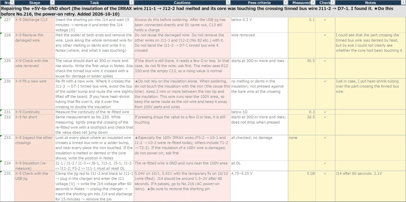
Rows added later to repair a short (some columns are hidden for readability). The yellow cells are my entries
We made it a rule that any test using AC100V would be written out step by step in the schedule, and carried out with me present.
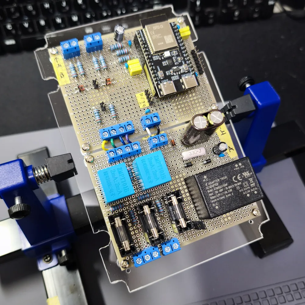
The two boards fixed to the acrylic plate. The signal board is on top, the primary board below
Machining the Parts #
Drilling the acrylic plate, case, and perfboards was done as follows:
- Print the machining drawings that Claude produced, to use as templates
- Stick each one on with 3M spray adhesive
- Rent a workspace at a home improvement store and do the machining
- Drilling with a drill press, cutting the outline of the acrylic plate, finishing with files, etc.
Fitting into the Case #
The two boards were fixed side by side on the acrylic plate and placed into the Takachi resin case.
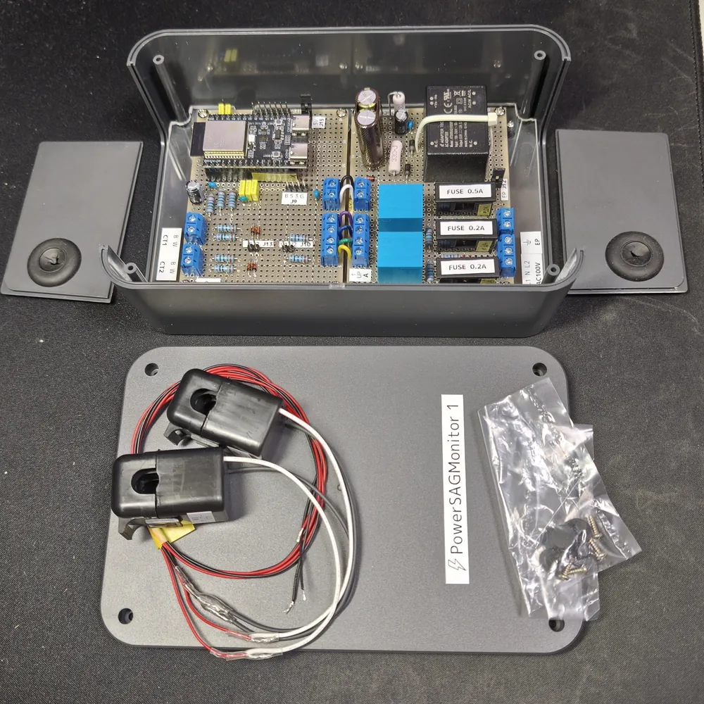
Inside the box. In front are the lid and the current sensors (CT)
Once assembled, the straight USB-C cable I tried to plug into the ESP32 microcontroller hit the EDLC on the neighboring board and would not go in. It is a pitfall that is hard to spot on a flat drawing. I happened to have a USB-C cable with an L-shaped connector, so that saved the day.
Installation at the Breaker Panel #
For voltage measurement and power, I added one branch breaker (BSHN2202). This is the only cable going into the box. Current is measured by clamping CTs around the main breaker’s wires. The CTs are the clamp-on type, so they can be attached without disconnecting existing wiring.
To stay safe, I switched off the main breaker and confirmed with a voltage tester and a multimeter that no voltage was present before working. I moved an existing 100V branch breaker to a different position and installed the BSHN2202 in the freed-up slot.
As an aside, I found several devices whose built-in clocks reset when the main power is completely cut: the water heater panel, the floor heating panel, and so on. Setting the clocks is tedious, so I do not want to do full power cuts very often.
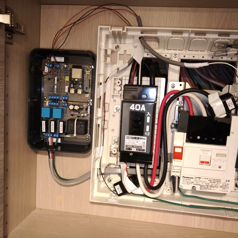
The box fixed to the left of the breaker panel (photographed with the lid and cover removed)
In the end, the PowerSAGMonitor box was fixed to the left of the breaker panel on October 17, and went into operation.
Troubles and Hard Parts During the Build #
Spray adhesive residue #
For the additional machining, I stuck printed templates on with spray adhesive. Everything went smoothly up to the machining, but when I peeled them off, sticky adhesive was left all over the boards and case, and it was a pain to remove. I found that rubbing with an eraser takes it off, and worked hard to clean it up.
Spray adhesive is hard to peel off, and apparently there is a separate spray made specifically for removing it. I did not buy it this time.
Needing lots of drill bits #
Claude’s original procedure specified hole diameters that differed by 0.1mm for each type of hole. I complained that “I can’t buy all those drill bits in sizes I’ll hardly ever use, and that are hard to find anyway,” and had them unified to some extent.
Drill bits in fine sizes around Φ1.x mm are not sold at home improvement stores.
Machining the acrylic plate #
Acrylic cracks easily and mistakes cannot be undone, so I was especially careful with the notches. For large holes, a step drill worked well.
The notches for screw clearance were very difficult and took the most time. Something like a laser cutter would have been nice, but I do not have access to one.
A “moving short” where 5V came and went #
In the AC100V power-on test, 5V on the output side of the power module sometimes appeared and sometimes did not. Repeating the same measurement gave different values.
| What I measured | Value |
|---|---|
| 5V line, with 33Ω in series on the USB jig (1st time) | 2.60V (normal) |
| Same measurement (2nd time) | 41–290mV |
| Resistance of the short | 0.3–2Ω |
The value changed every time: a so-called “moving short.” Suspecting a marginal short somewhere, I checked visually many times. Eventually, as shown in the photo, I found a spot where the insulation of a GND insulated wire had been dented by heat, and was suspected of touching the crossing +5V tinned bus wire.
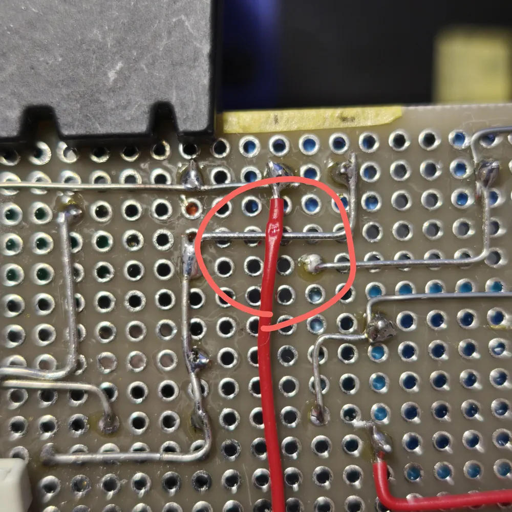
The problem crossing is inside the red circle. The insulation of the GND wire is dented
Visually, I could not really tell whether the core was actually touching.
For now, I redid the insulated wire and put heat-shrink tubing over the crossing just in case. That seems to have worked: after rewiring, the USB power jig test gave 5.08V, and the output of the power module connected to AC gave 4.60V (4.73V after 10 minutes).
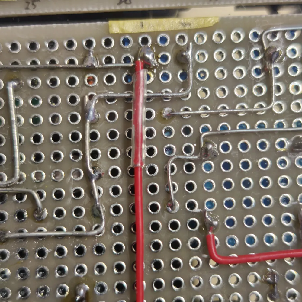
After rewiring. Heat-shrink tubing covers the crossing
Misdiagnosing the power module as “broken” #
With the 5V problem above, before the wiring issue was found, Claude judged the power module to be “broken” based only on the resistance on its output side, so I bought another power module.
It turned out that solder had not been wetting the power module’s pins either. When I tested the part that had been removed as “broken” using IC clips, it put out 5V. After polishing the pin surfaces with a file and applying flux, solder started to wet them.
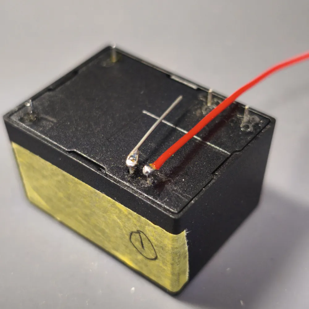
I polished the pins of the removed module and tested how solder wetted them
Maybe it had been in stock for a long time and the pins had oxidized.
Current readings only 40% of actual #
When I checked the current readings with a hair dryer, they came out at only about 40% of the clamp meter’s value. The cause was that the joint of the clamp-type current sensor was not fully closed. New CT modules have extremely stiff joints, so this is easy to miss.
| Clamp meter | Box reading | Voltage drop | |
|---|---|---|---|
| Before fixing | 11.7A | 4.93A (42%) | 101.36 → 96.99V |
| After fixing | 11.4A | 11.30A (−1%) | 102.22 → 97.62V |
The voltage drop is nearly the same both times, which shows that the dryer was drawing the same current and only the reading was low.
A mirrored outline drawing #
The holes in a perfboard are on a 0.1-inch (2.54mm) grid, but some parts, like the fuse sockets and the power module, have pin spacing that does not match. I drilled additional holes for those parts based on the machining drawings Claude produced. I did that work in the rental workspace at a home improvement store.
When I got home and started mounting parts, not a single pin of the power module went into its holes. Comparing them, the extra holes I had drilled were laid out the reverse way, front to back. When I asked Claude, the cause turned out to be that the power module’s outline drawing was a “view from the bottom,” but it had been used without mirroring left to right. On the same drawing, the voltage sensors had been mirrored, but when the power module was added later, the same procedure was not followed.
Claude looked for a placement that would not collide with the holes already drilled, and placed the power module again rotated 180°. Three of the four holes drilled for the power module could be used as-is, and only two extra holes were needed. I drilled those two with a pin vise (a small hand-turned drill), and avoided remaking the board. The lessons: “Check which side an outline drawing is viewed from” and “Hold the real part against the template before drilling.”
A gap in the automatic checks of the wiring layout #
The wiring routes in the physical wiring layout are laid out automatically by Claude’s script. There are two rules for the routes:
- Bare wire only passes over lands (the round copper pads you solder to) of the same circuit, or unused lands. If there is a land of another circuit in the way, it detours, and if it cannot get through, it becomes insulated wire
- Insulated wire may cross over other lands and wires
The results were also checked with KiCad’s DRC, but there was a gap here. To allow insulated wire to cross, we had disabled DRC’s “short” rule, so even if bare wire landed on another circuit’s land, DRC would not catch it.
If a bug in the script had laid out such a route and the wiring layout had gone out without anyone noticing, then as soon as I wired it as drawn, the bare wire would have been soldered to another part’s pin, causing a short. This gap was discovered when I reviewed the wiring and changed some of it to insulated wire, and a warning that had been appearing for a different reason disappeared. Claude added a check that counts whether any bare wire lies on a land of another circuit, so this can be confirmed at the drawing stage, before wiring. When we ran the new check, it turned out there were no such routes in reality.
The GND split existed only on paper #
A perfboard has no GND plane (a solid ground area) like a printed circuit board; the current return paths are individual tinned bus wires. The microcontroller draws a large current (up to about 300mA) every time it transmits over Zigbee, so if that return path shares the same wire as the reference for the analog signals, a small error gets added to the measured values. So Claude decided to split GND into three branches (power, 3.3V, analog) and gather them separately at the microcontroller’s three GND pins (star wiring). The three GND pins are connected inside the microcontroller module.
However, when I looked at the generated wiring layout, the branches seemed to be mixed together. Claude investigated and found that this was indeed the case. Since all three branches are the same GND circuit, bare wire could pass over lands of another branch. The analog branch’s bare wire stepped on a land of the 3.3V branch, and on the board they were joined into one.
Claude added a rule when laying out routes: “even for the same GND, do not land on another branch’s land,” and made it check every time that the finished bare wires are split into three. The lesson: “Even if you think you split them, they are not split until you check the routes too.”
That said, according to the design estimates, this error is an order of magnitude smaller than the ADC’s own error. The star wiring was not done because the device would not work otherwise, but because it was an improvement that could be had for little effort.
Coming Up Next #
Part 3 (Operation) covers integration with Home Assistant and firmware tuning. It will cover how over-the-air firmware updates were cut from 47 minutes to 3 minutes, and how the reason Wi-Fi could not be used turned out to be drift in the microcontroller’s crystal.